FESEM/FESEM with EDS
| Make: | TESCAN and Bruker |
| Model: | MIRA 3 ( FESEM) and Quantax 200 (EDS), Evactron XEI (plasma cleaner) |
| Year of purchase: | 2014 (FESEM –EDS), 2016 (Decontaminator) |
| Funded by: | |
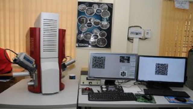
| Location: | TEM/SEM Lab |
| Contact email: | semlab@cens.res.in |
| Book New Request | |
- 2X to 10,00,000X Magnification
- High vacuum and low vacuum ( up to 500 Pa) imaging
- IR camera for chamber view
- Everhart-Thornley type detectors with YAG scintillators
- Chamber SE detector, Resolution-1.2 nm at 30 kV (SE: Secondary electrons)
- In-Beam SE detector,Resolution-1.0 nm at 30 kV
- Pneumatic anti-vibration suspension system
- Accelerating voltage- 50 V to 30 kV in steps of 10 V
- Probe current 2 pA to 200 nA
- Field of view- 6.4 mm at WD 10 mm and 20 mm at WD 30 mm
- 20 ns to 10 ms per pixel scanning speed (Adjustable continuously)
- Selectable image frame size up to 8192 X 8192 pixels
- Point & line scan, image rotation & shift and tilt compensation
- Sample stage movements : Motorized X,Y,Z = 80 mm, 60 mm, 47 mm respectively
- Rotation = 360 deg –motorized
- Tilt = -80o to +80o –motorized
- Energy Dispersive X-ray Spectrometer (EDS)-having Peltier cooled Silicon drift detector (SDD)
- Detection from Boron (5) to Americium (95)
- Maximum input count Rate > 1000 kcps
- 30 mm2 Active Area
- Resolution < 129 eV (MnKalpha)
- ESPRIT Quant-automatic software tools for standard less quantitative spectra analysis
- Image acquisition from SE source
- Multi point, line scan and mapping (ultra fast digital elemental mapping with unlimited number of elements), histograms, binary and ternary charts
- Secondary electron imaging for morphology studies
- Backscattered electron imaging
- Low vacuum detector for imaging non conducting materials.
- Scanning Transmission Electron Microscopy (STEM) at 30 kV with 2 detectors TE bright and TE Dark
- Beam deceleration mode
- Decontaminator attachment for plasma cleaning of sample surfaces and chamber
- EDS quantitative spectra analysis
- EDS mapping of various elements
| Modes | Duration (hrs) |
|---|---|
| EDS | 15 min per sample |
| STEM | Usually takes 5 min (It depends on the scan rate) |
| High Vacuum | 1 hour per sample |
| Low vacuum (LVSTD) | 1 hour per sample |
| Sl. No. - Category | Fees ( in Rs/- ) + additional 18% GST |
|---|---|
| 01 - Academic Institutes | 1200 (1700 for Au sputtering) per slot / 1 hr |
| 03 - External Industry Users | 2400 (3400 for Au sputtering) per slot / 1 hr |
| 02 - External Industry Partner | 1800 (2550 for Au sputtering) per slot / 1 hr |